A recent trial user had an application that required creation of a three-dimensional mesh of a printed circuit. Such an object is thin in z with relatively complex spatial variations in x-y. The user attempted to represent the full complement of conductors as a single, thin STL solid object with thousands of facets. It would have been astronomically difficult for MetaMesh to analyze such a structure. The task is equivalent to deciding whether a point is inside or outside a thread of a spider web.
In reviewing the application, it occurred to me that there was a much easier approach to model such a structure, based on technology that we had already incorporated in the two-dimensional Mesh program. The idea is to assign elements in a plane to regions according to values in a photographic image. The advantages are easy setup and high reliability. In this article, I will describe new MetaMesh capabilities for analyzing photographs and illustrate them with an example of a layer in a printed circuit.

Figure 1. Sample printed circuit, PNG format.
Figure 1 is a photograph of the test geometry. The image has only two colors — white represents thin conductors. In the benchmark example, conductors (Region 2) are mapped to a 1.0 mm layer in a uniform solution volume (air, Region 1). The first step is to set the interpretation of photographs. The following entries appear in the GLOBAL section of the MetaMesh script:
INTERVALS Lightness
  50.0? 100.0? 2
END
The construct states that photographs will be interpreted in terms of lightness values (0.0 to 100.0 percent). Lighter areas will be assigned to Region 2. An INTERVAL section may contain up to 250 data lines — in this case, only one interval is needed. Alternatively, assignment may be via hue values (0.0 to 360.0 degrees) in the image.
Parts are basic building blocks in MetaMesh. The concept is flexible — parts range from simple geometric solids to complex STL shapes. We have added a new PHOTO part type. The following section defines a photo part in the example:
PART
  Type Photo PC01.PNG 0.00 0.00 50.00 50.00
  Name PC
  Fab 1.00
END
In the workbench frame, the photograph image is mapped into an x-y plane centered at z = 0.0 with thickness ?z set by the fabrication parameter. The resulting solid can be moved to any position or orientation with optional SHIFT and ROTATE commands. In the example, the photographic image is contain in the file PC01.PNG. (MetaMesh also handles BMP and PCX formats.) The information is mapped to an area with spatial dimensions xmin = 0.0, ymin = 0.0, xmax = 50.0 and ymax = 50.0, independent of the image pixel dimensions. Figure 2 shows the resulting mesh in the slice plane z = 0.0, while Figure 3 shows a three view with perspective. The entire structure was created with the two simple statements listed above.
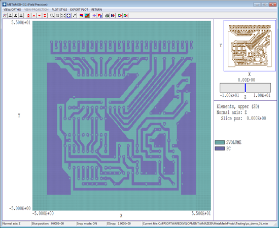
Figure 2. MetaMesh screen shot, slice in the plane z = 0.0.
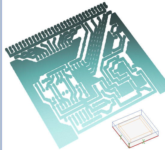
Figure 3. Three dimensional view, printed-circuit example.
Photographic analysis is a powerful new feature of MetaMesh. It greatly simplifies the representation of multi-layer printed circuits and striplines for electromagnetic analysis. Complex printed-circuit assemblies can be built in two steps:
- Set up a foundation mesh with element layers of the appropriate thicknesses.
- Use photographic layouts to set conductors or dielectrics in each layer. If there are different components in a single layer, they can be represented with different colors in the photograph.
The photographic method has unlimited applications. Information from up to 250 photographs may be included in a MetaMesh script. The technique applies to any three-dimensional structure with photographic slice data, such as MRI scans.
LINKS
